


E-Reticle™
產品查詢In the process of semiconductor manufacturing, a production reticle passes through many stations and treatment processes in which it can be exposed to external electric fields or where charges can emerge on the glass surfaces of the edges and backsides or charge carriers can transferred to the Chrome ring through contact. Even in manufacturing processes with well engineered electrostatic protection concepts, there are always areas in which electric fields can affect the reticle or where charges can remain for long time on the glass surface of reticles.
The measurement of electric fields in the manufacturing of semiconductor components is a tricky thing and it is difficult to obtain realistic and reliable data regarding the endangering electrostatic potentials and local field strengths at all locations in the production environment.
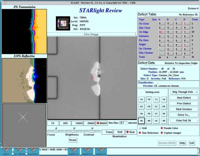
ESD damage at a reticle chrome-line, detected by a “KLA-TENCOR Starlight inspection tool"
Even when one succeeds by using a suitable measuring device to measure the ambient field intensity at all locations through which the reticle normally passes, from the goods receiving area through the visual inspection stations, the inspection machines, the handling robots, the stockers, along the sometimes very long routes of the transportation systems, within the steppers in the buffers, the libraries, at the ID reader, at the exposure stages, in the cleaning systems, etc., it cannot be guaranteed that the measured values will apply under normal manufacturing conditions, particularly when the reticle itself is present.
The situation for the mask manufacturer is even more critical. The complexity of the process there is much higher as in the case of the reticle users and the risk that the reticle will be exposed to strong electric fields at some manufacturing step is here much higher. The production environment even with a high level of automation is subjected to constant changes, and also the products over time become more sensitive to the electrostatic dangers because the CDs are becoming smaller and smaller.
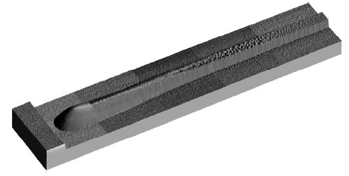
Degraded reticle Chrome-line due to EFM (electric field induced migration of Chrome) under the influence of electrostatic charges far below the ESD threshold.
Therefore, continuous control over hazardous electrostatic potentials for reticles in the semiconductor production process or in mask manufacturing must also be an absolutely necessary quality assurance measure. However, since no reasonably suitable direct measurement method is available, it can always happen that ESD damage occurs unexpectedly on a production reticle.
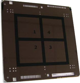
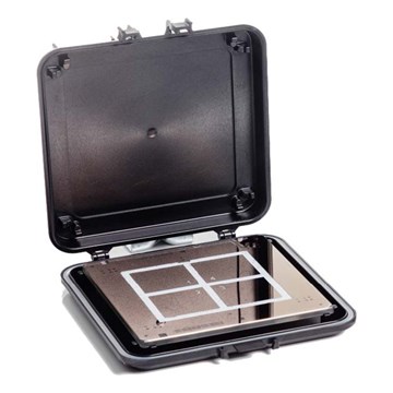
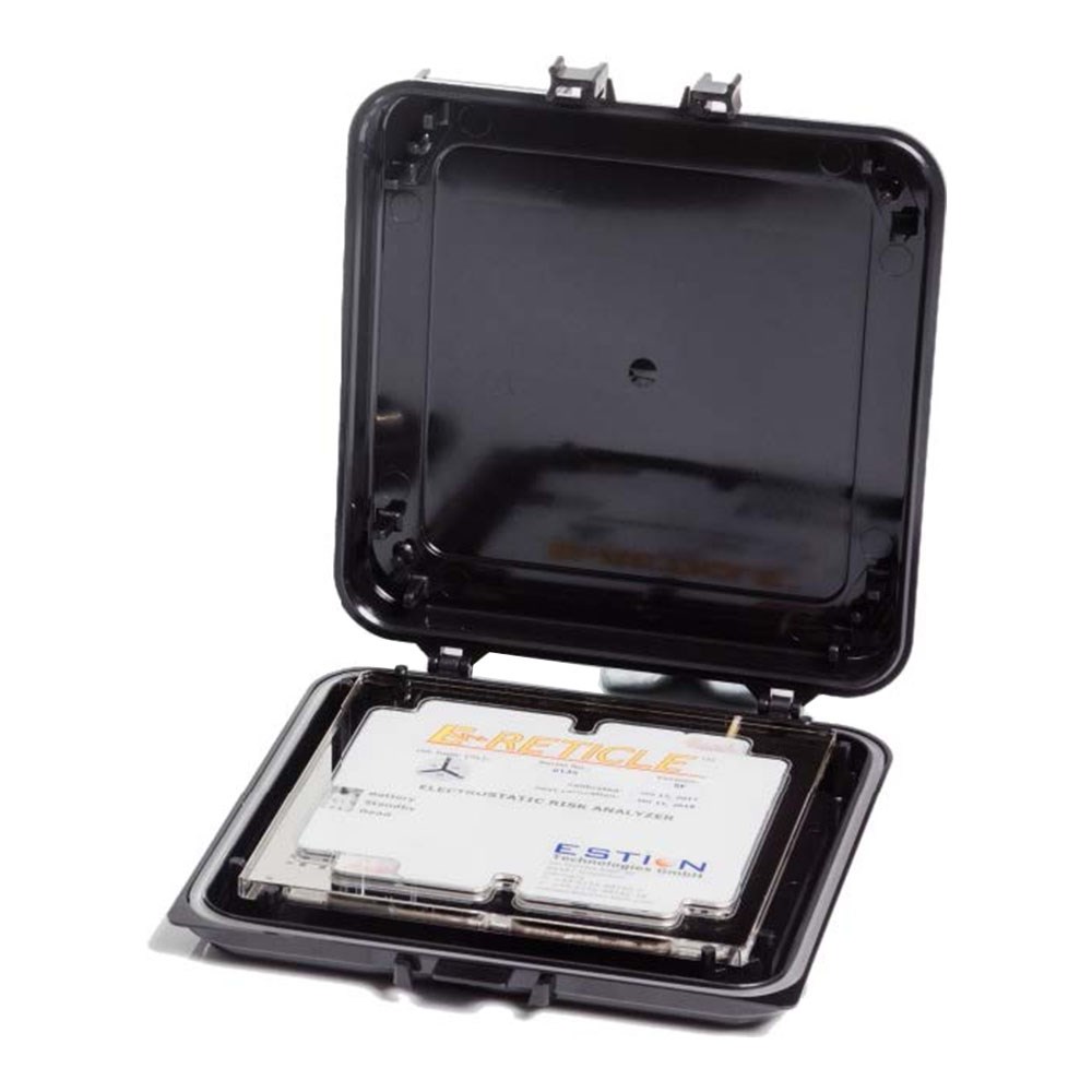
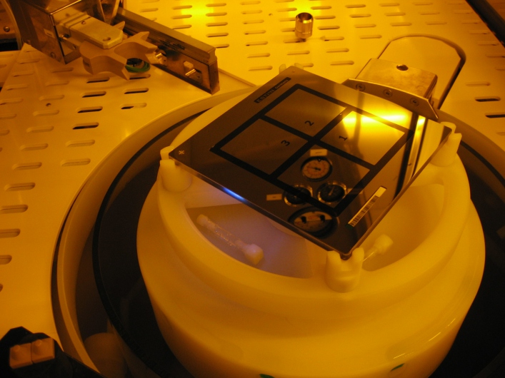
The E-RETICLETM consists of a quartz casing with the outside dimensions of a SEMI standard 6" reticle. A 100 nm thick Chrome structure with AR coating is mounted on the front side of the quartz body.
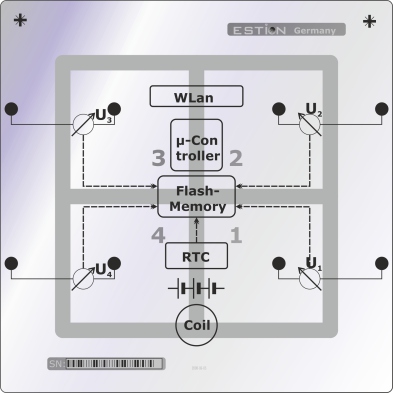
Within the E-RETICLETM quartz glass casing, there are 4 electrostatic voltmeters which measure the electric potential difference between 4 segments and the Chrome-ring. These values can be converted to critical field-strengths. A real-time clock in the device assigns the clock time to the measured values. The measured values along with the clock times assigned to them are loaded in a memory with a selectable sampling rate of 5-20 Hz.
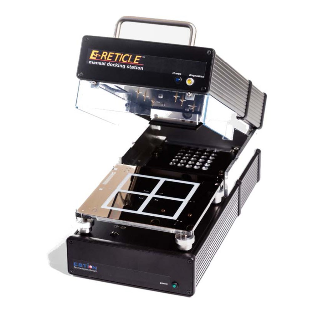
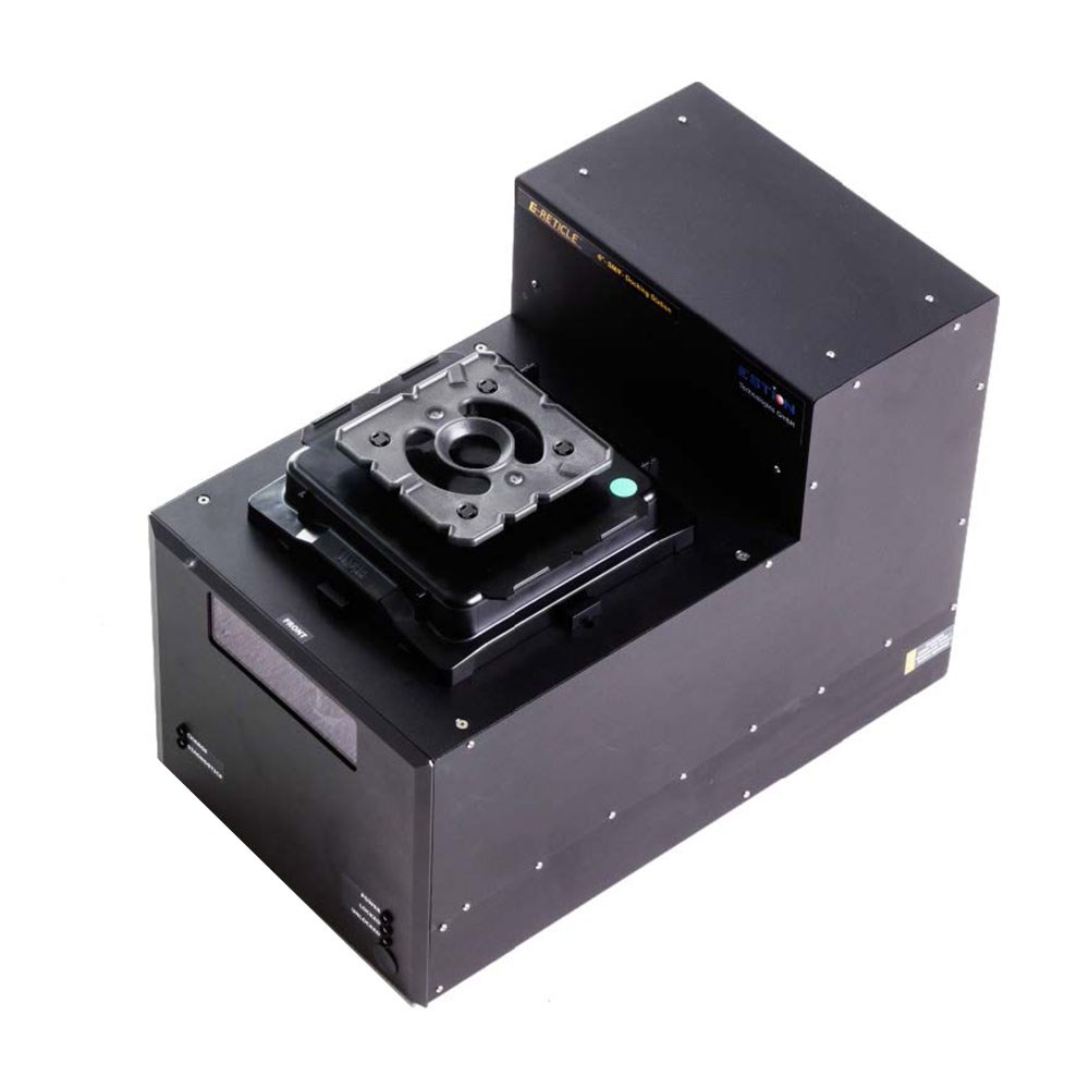
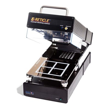
A wifi transceiver is also located within the E-RETICLETM and the counterpart is in a 8" or 6" SMIF-docking station which can receive the measurement reticle and has additional functions as the battery charger via induction, neutralizing and zero-adjust.
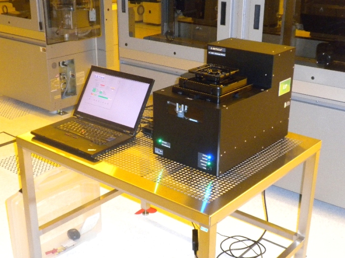
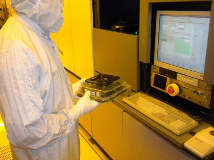
The measurement process can be started from the docking station, and then the E-RETICLETM can be exposed for up to about 6 hours to the measurement handling processes as well as to the semiconductor manufacturing processes or to a large part of the mask manufacturing processes. The mask-house version is hermetically sealed and can be immersed.
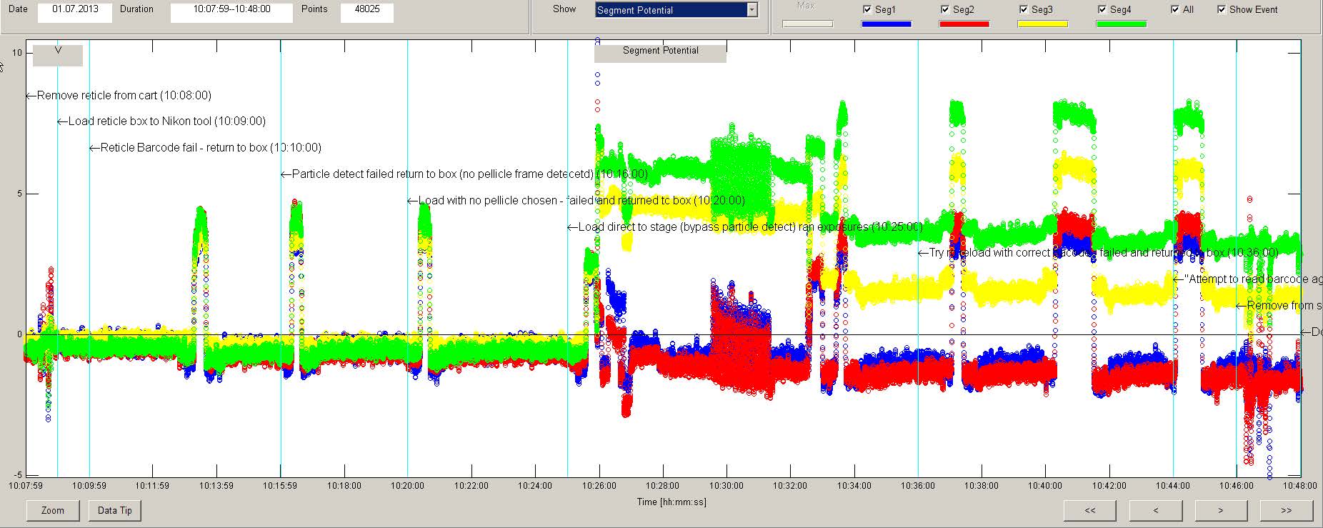
The measurement data can be transferred per low-power wifi from the E-RETICLETM to a PC where they can be evaluated with a specific analyzes software.
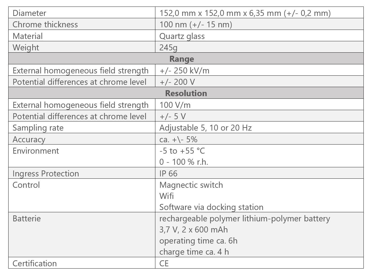
Specifications: