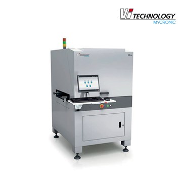
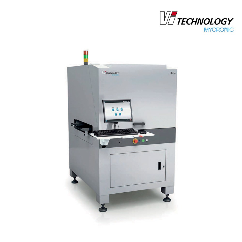
K Series 3D AOI
產品查詢Take inspection to another dimension

Features:
Powerful 3D AOI
Drill down into powerful image library tools with advanced algorithmic assistance.
Precise optical metrology
High-precision metrology combining high-definition 2D texture with shadow-free 3D inspection that eliminates image cropping and warpage effects.
Complete test coverage
Comprehensive defect coverage accurately measures component body and solder joints to identify misplaced components, tombstones, lifted leads and more.
Specifications:
| Specifications | 5K | 8K | 9K |
| Defetcs test coverage | Presence/absence, positioning X/Y/Ө/Z, tombstone, polarity, coplanarity, upside-down components, OCR/OCV, solder joints, lifted leads, head-in-pillow, pins & critical distance measurements, foreign materials detection, IPC 610 compliance verification | ||
| Z reconstruction range | -5 / 20mm | ||
| Conveying height | 860-960 mm | ||
| Minimum PCB dimensions (L x W) |
2" x 2" (51 x 51 mm) | 2" x 2" (51 x 51 mm) | 2" x 2" (51 x 51 mm) |
| Maximum PCB dimensions (L x W) |
21" x 24" (533 x 609mm) | DL: 2
x (17" x 12.8") (2 x (432 x 325) mm) or 2 x (21" x 11.0") (2 x (533 x 280) mm) |
21" x
24" (533.4 x 609.6 mm) |
| DL: Dual Lane mode | 37" x 24"
(option) (939 x 609 mm) |
||
| SL: Single Lane mode | SL
: 1 x (17" x 23.6") (1 x (432 x 600) mm ) or 1 x (21" x 23.6") (1 x (533 x 600) mm) |
||
| PCB thickness | 0.5 - 4 mm | 0.5 - 4 mm | 0.5 - 15 mm |
| Maximum PCB weight | 3 kg | 3 kg | 15 kg |
| Minimum edge clearance | 3 mm | 3 mm | 4 mm |
| Top clearance | 34 mm | ||
| Bottom clearance | 60 mm | ||