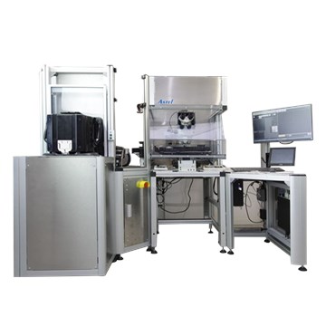
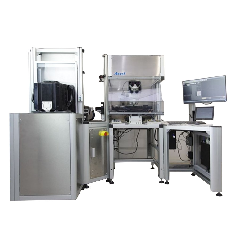
SIL12000 Wafer Loader / MIL 12000 Wafer Inspection System
製品のお問い合わせSIL12000 is an automatic loading system for silicon wafers from FOUP carriers, to be used on Leica DM12000 or other inspection microscopes. MIL12000, with the same loading mechanism, includes MACRO inspection with a collimated light source to complete the inspection options
Features:
- Unique FOUP loading system for cost-effective and fast wafer loading
- Mechanical structure with linear motion and rotation for safe handling
- The architecture ensures safe and fast operation with high process cleanliness
- PC system with a user-friendly touchscreen interface
- Software with recipe management for easy switching between wafer sizes and thicknesses
- Various wafer selection methods for versatile inspection needs
- Compatible with SEMI standard FOUP carriers, with automatic carrier opening
- Ability to handle manually opened FOSB carriers and 200 mm carriers with an adapter kit
- Auto recipe tool for defining new cassette profiles
- Default safety features: laser mapping, cross-slot detection, wafer protrusion
- Optional microscope rotating chuck with notch finder
- The SIL version includes optical centering, an alignment system, and a macro inspection unit for front inspection
- MIL version can be interfaced with the RWMAP system for complete defect review and wafer map management
- Optional mini environment hood with laminar flow and filtering unit for sensitive applications
Specifications:
| Wafer Thickness | • 12” from 600μm - 1000 μm (Standard) • 8” from 200 μm - 1000 μm • Other thickness on request |
Throughput | • Up to 100 Wafers per Hour |
| Wafer Size | • 8”, 12” • Double wafer size version with a 200mm adapter kit |
Environment | • Class ISO4 (ISO EN14644) • CE Mark • SEMI Standard Compliant |
| Wafer Types | • Silicon (Si) • Sapphire (Al2O3) • Glass • Ceramic |
Safety Features | • Cross-slot Detection • Laser Mapping with Wafer Thickness and Distance Measurement • Wafer Protrusion Alarm • Faults Detection (Electrical, Vacuum, Air) |
| User Interface | • Windows 7 • 8” TFT Touch Screen |
Networking | • SMB (Windows Networking) • SECS-GEM (Option) |
| Communication Ports | • Ethernet • USB |
Footprint | • 1800 (W) x 1200 (D) x 1350 (H) mm |
| Handling | • High-reliability Carbon Fiber End Effector • Mechanical wafer recentering • Cassette laser mapping |
Options | • Optical centering unit • Rotating microscope chuck with notch finder • MACRO Inspection of the unit with LED light source • 200mm carrier handling kit • Mini environment hood |
| Inspection Modes | • All Wafers • Selected from a recipe • Direct selection • Statistical Mode |
Carrier Type | • 300mm SEMI Standard FOUP carriers • 200mm SEMI Standard carriers with adapter |