

E-Wafer™
產品查詢In the process of semiconductor manufacturing, a production wafer passes through many process steps where it can be exposed to external electric fields which induce potential differences. Electrostatic charges can be created on the surface due to friction or imbalanced ionizers. Even in manufacturing processes with well engineered electrostatic protection concepts, there are always areas in which electric fields can affect the wafer or where charges can remain for long time on isolated surfaces.
The measurement of electric fields or electrostatic charges in the highly automated manufacturing of semiconductor components is tricky. It is difficult to obtain realistic and reliable data regarding the endangering electrostatic potentials and local field strengths at all locations in the production environment.

Even when one succeeds by using a suitable measuring device to measure the ambient field intensity at all locations through which the wafer normally passes, from the goods receiving area through visual inspection stations, handling robots, stockers, transportation systems etc., it cannot be guaranteed that the measured values will apply under normal manufacturing conditions, particularly when the wafer itself is present.
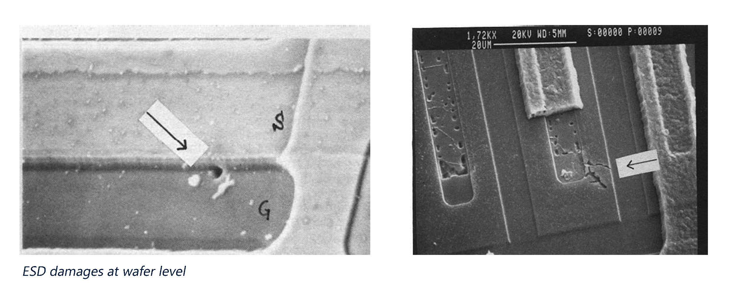
The situation inside the production tools is even more critical. Numerous friction processes happen during the wafer manufacturing, potentially creating critical electrostatic charges and on the wafer. Clamping and unclamping on vacuum chucks or electrostatic chucks, friction between liquids and wafer surfaces in cleaning processes, and interactions between gases and the wafer surface are well known risk factors. These charges can creat ESD events, non-uniform surface conditions, or increased particle deposition.
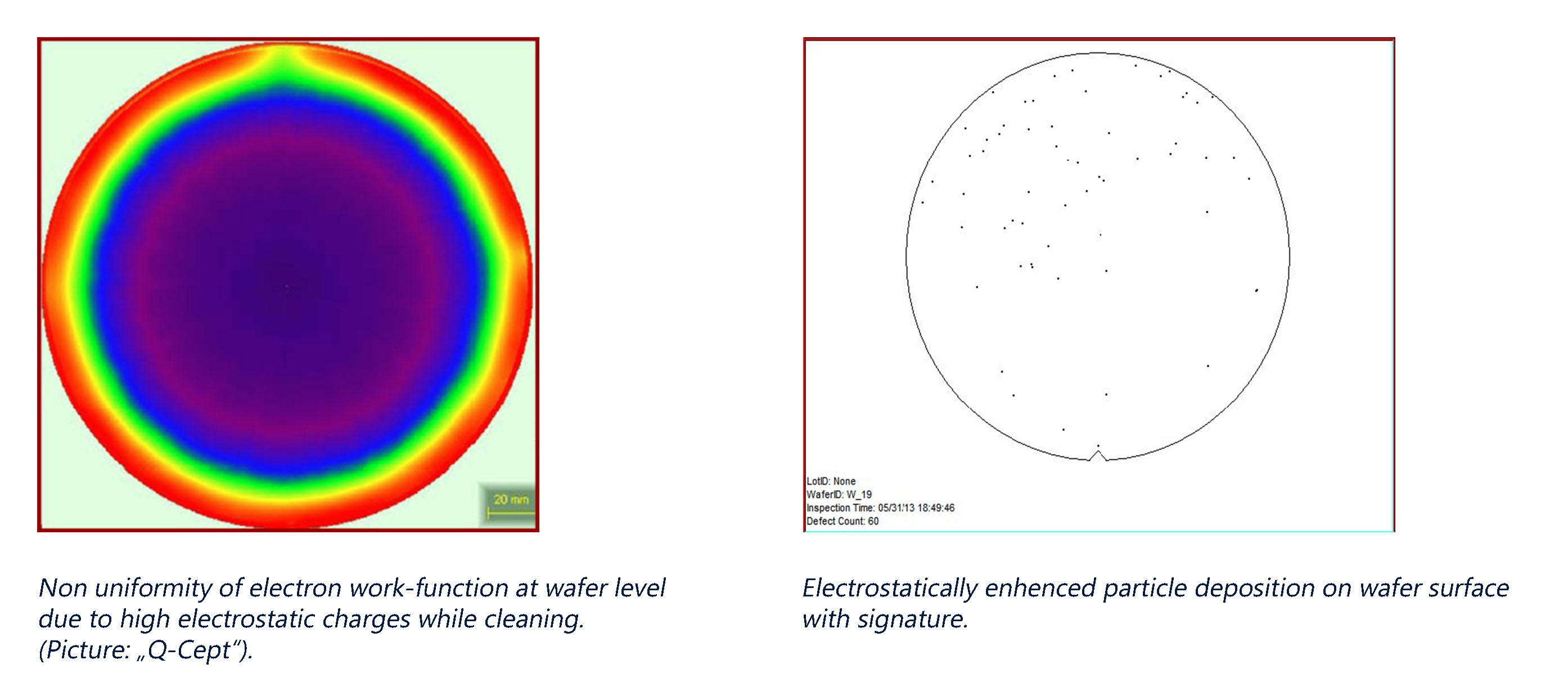
Therefore, continuous control over hazardous electrostatic potentials for wafers in semiconductor production is an absolute necessity quality assurance measure. However, since no reasonably suitable direct measurement method has been available until now, it could always happen that ESD damage occurs unexpectedly.
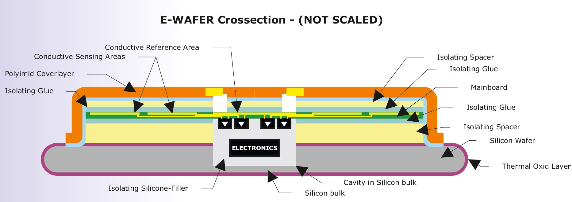
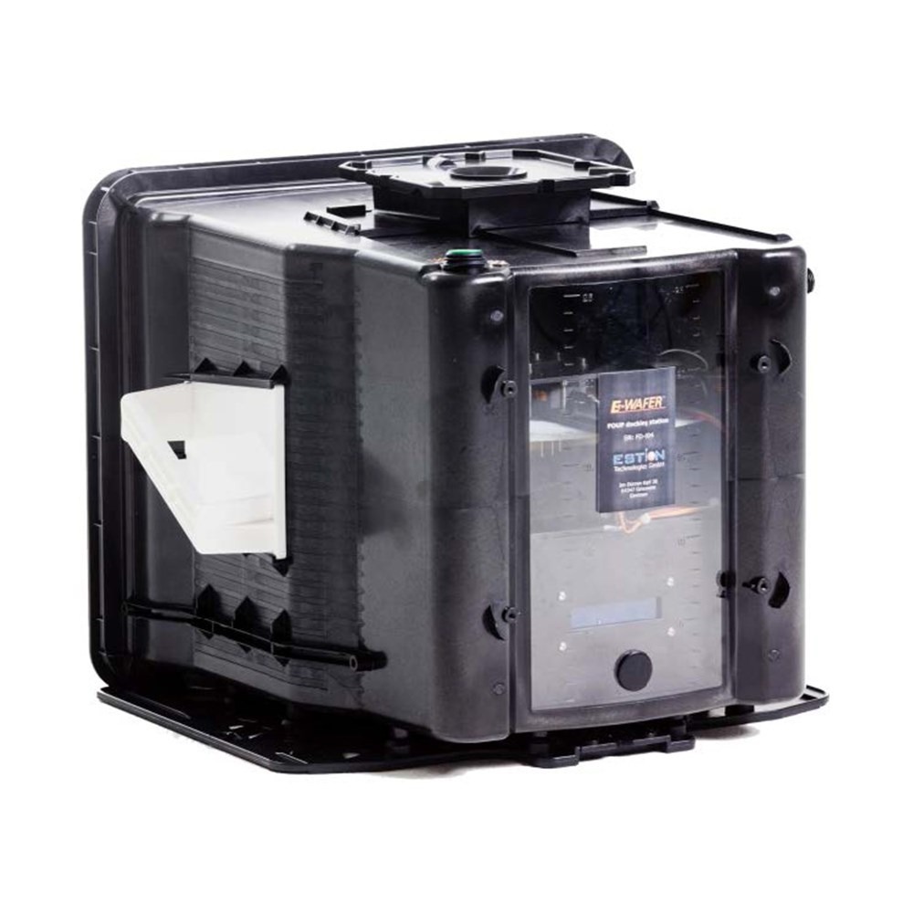
E-WAFERTM is made from a 200mm or 300mm Silicon wafers with a thermal oxide layer. Eight sensing areas are distribute concentrically over the wafer surface and placed on top of the oxide layer. The center area contains the entire electronics and battery and is partly embedded into the bulk silicon. The entire measuring system is hermetically covered with a polyimid layer.
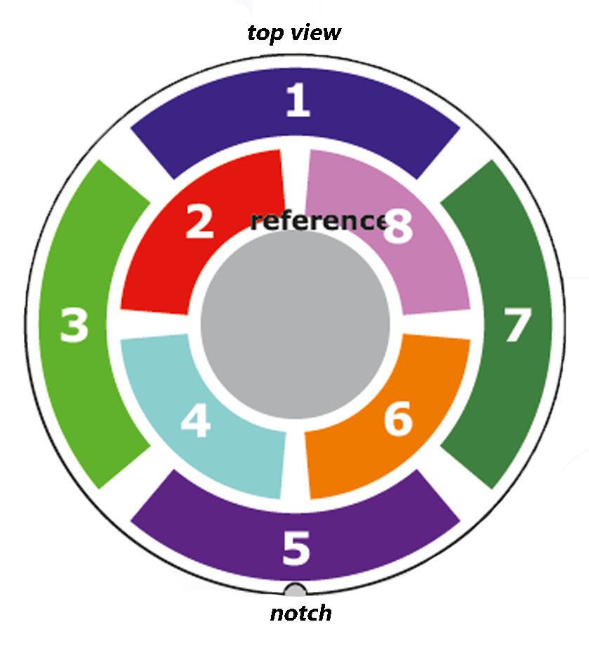
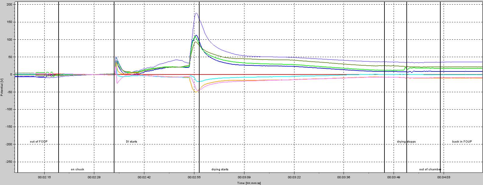
Within the E-WAFERTM, there are 8 electrostatic voltmeters which measure the electric potential difference between 8 segments and the center area. These values can be converted to critical field-strengths. A clock in the device assigns the clock time to the measured values. The measured values along with the clock times assigned to them are loaded in a memory with a sampling rate of 10 Hz.
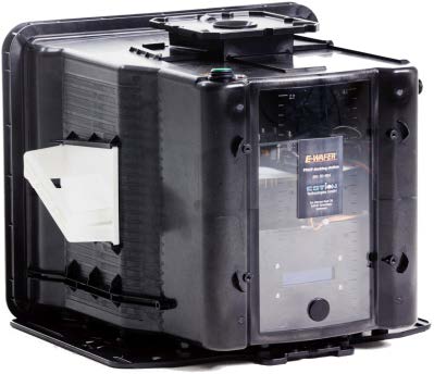
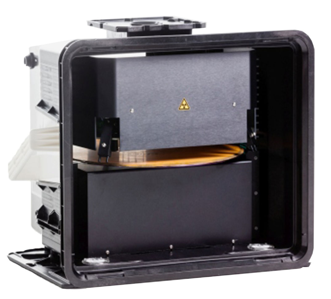
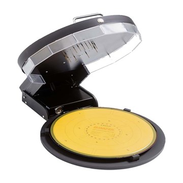
Battery charging, communications, data transfer, neutralizing and zeroing is done via special switchable contacts inside a docking station. For 300mm E-WAFERTM the docking station is integrated into a SEMI-standard FOUP with a USB communication port. Alternatively there is a portable docking station adaptable for 200mm and 300mm EWAFERTM.
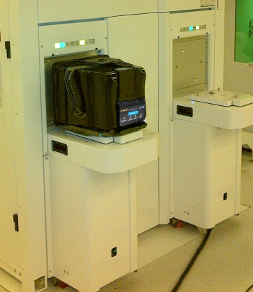
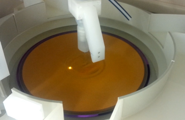
The FOUP-docking station can be handled and placed on the tools as a standard production FOUP. The measurement starts from this FOUP docking, and then the E-WAFERTM can be exposed for up to about 2 hours to the manufacturing processes of interest . The system is hermetically sealed and can be immersed in wet processes.
The measurement data from E-WAFERTM can be transferred to a PC where they can be evaluated with a specific analysis software. Process logfiles can be synchronized.
Specifications: